This article is part of my series of projects around Ternary Computing and Processor Design. Click here to see the list of projects of this series.
Abstract – Ternary logic is an alternative to binary logic used in every modern processor. As a base-3 numerical system can represent numbers using fewer digits than in base-2, ternary logic circuits are theorized to be more compact than equivalent binary circuits. This increase in density could lead to a gain in performance measured in transistor cost, maximal frequency and energy consumption. In this project, the details of balanced ternary algebra are reviewed and a ternary Arithmetic Logic Unit (ALU) is designed and built using CMOS chips to prove the feasibility of large ternary CMOS circuits. Finally, a theoretical analysis of the benefits of balanced ternary logic is presented. The conservative conclusion of this analysis is that balanced ternary can be cheaper and faster than equivalent basic binary logic, however, binary logic has decades of optimization tricks making it way cheaper and faster.
Keywords – ternary computing, processor architecture, ALU design, many-valued logic
Introduction
Motivation
Every modern computer uses binary logic, 1s and 0s, for computations. Theoretically, any numerical base can be used for computation [1]. The numerical base (or radix) defines how many digits will be necessary to represent a certain number, this is the radix economy and is written as $$E(b,N)$$ for base $$b$$ and number $$N$$ and calculated with the following formula. ££ E(b,N) = b \lfloor 1+log_b N \rfloor££
The lowest average radix economy is reached for base $$e \approx 2.72$$ [2]. The closest integer base is $$3$$, not $$2$$ ; ternary not binary, and leads on average to the smallest radix economy.
Therefore, a computer using ternary logic could be more efficient by requiring less digits and less circuitry for a similarly powerful processor. The most famous ternary computer was the Setun made by the soviets in the 1970s and was more efficient [3]. However, binary processors are easier to develop and binary won. As Moore's law slows down, it might be time to bring ternary computing back to gain performance.
Switching to ternary logic requires redefining a whole new algebra, and a more complex one as the number of possible states and thus gates is larger.
Ternary algebra
Ternary values
As the binary set of values is written $$\mathbb{B}=\{0,1\}$$, the symbol $$\mathbb{T}$$ will be used for the set of ternary values. There exist multiple ternary sets of values and thus multiple algebras : perhaps the most obvious is unbalanced ternary with $$\mathbb{T}=\{0,1,2\}$$ ; unknown-state ternary with $$\mathbb{T}=\{F,?,T\}$$ similar to an epistemological set of truth values and an extension of the Boolean True-False interpretation of binary logic ; and balanced ternary $$\mathbb{T}=\{-,0,+\}$$ [4].
Balanced ternary logic will be used in this report. It allows operations on negative and positive numbers by default with-out having to use the ternary equivalent of two’s complement. Consequently, if we only use the positive numbers, the range of possible values is halved. This choice benefits unsigned operations over signed operations.
In practice on an electrical computer, balanced ternary would be represented by positive, negative and zero voltage. Exotic ternary computers could use micro-fluid direction or light polarization. The use of ternary logic for quantum computation will not be discussed in this report.
Analogous to the binary 8-bit byte and 4-bit nibble, a 3-trit word can be called a tribble and a 9-trit word a tryte. The word tryte has also been used for a smaller 6-trit word, but does not follow powers of 3. A byte is two nibbles. A tryte is three tribbles.
One-input gates
In binary, a gate with one input and one output can be represented as a two by one matrix.
| Input | Output |
|---|---|
| 0 | 1 |
| 1 | 0 |
Can be written with the matrix ££ \begin{bmatrix} 1\\ 0 \end{bmatrix} ££
Therefore there are $$2^2=4$$ possible one-input one-output matrices in binary :
| Matrix | Schematic | Description | Name |
|---|---|---|---|
| $$ \begin{bmatrix} 0\\ 0 \end{bmatrix} $$ | Clear | CLR | |
| $$ \begin{bmatrix} 1\\ 1 \end{bmatrix} $$ | Mark | MRK | |
| $$ \begin{bmatrix} 0\\ 1 \end{bmatrix} $$ | Identity, buffer or pass | BUF | |
| $$ \begin{bmatrix} 1\\ 0 \end{bmatrix} $$ |  |
Inverter | NOT |
Table 1 : binary one-input gates
Only the last two are useful.
In ternary logic, one-input one-output gates can be represented with a three by one matrix. There are $$3^3=27$$ possible such gates. Here are the meaningful ones [5].
| Matrix | Schematic | Description | Name | Symbol |
|---|---|---|---|---|
| $$ \begin{bmatrix} -\\ 0\\ + \end{bmatrix} $$ |  |
Identity, buffer or pass | BUF | $$A$$ |
| $$ \begin{bmatrix} +\\ 0\\ - \end{bmatrix} $$ |  |
Inverter | NOT | $$\overline A$$ |
| $$ \begin{bmatrix} +\\ +\\ - \end{bmatrix} $$ |  |
Positively biased inverter | PNOT | $$\hat{A}$$ |
| $$ \begin{bmatrix} +\\ -\\ - \end{bmatrix} $$ |  |
Negatively biased inverter | NNOT | $$\check{A}$$ |
| $$ \begin{bmatrix} +\\ 0\\ + \end{bmatrix} $$ |  |
Absolute value | ABS | $$|A|$$ |
| $$ \begin{bmatrix} 0\\ 0\\ + \end{bmatrix} $$ |  |
Clamp up | CLU | $$\left \lceil{A}\right \rceil$$ |
| $$ \begin{bmatrix} -\\ 0\\ 0 \end{bmatrix} $$ |  |
Clamp down | CLD | $$\left \lfloor{A}\right \rfloor$$ |
| $$ \begin{bmatrix} 0\\ +\\ + \end{bmatrix} $$ |  |
Increment | INC | $$A^{+}$$ |
| $$ \begin{bmatrix} -\\ -\\ 0 \end{bmatrix} $$ |  |
Decrement | DEC | $$A^{-}$$ |
| $$ \begin{bmatrix} 0\\ +\\ - \end{bmatrix} $$ |  |
Rotate up | RTU | $$A$$╯ |
| $$ \begin{bmatrix} +\\ -\\ 0 \end{bmatrix} $$ |  |
Rotate down | RTD | $$A$$╮ |
| $$ \begin{bmatrix} 0\\ 0\\ + \end{bmatrix} $$ |  |
Is positive | ISP | $$A^{=+}$$ |
| $$ \begin{bmatrix} 0\\ +\\ 0 \end{bmatrix} $$ |  |
Is zero | ISZ | $$A^{=0}$$ |
| $$ \begin{bmatrix} +\\ 0\\ 0 \end{bmatrix} $$ |  |
Is negative | ISN | $$A^{=-}$$ |
Table 2 : ternary one-input gates
Most of them are only useful in rare situations when building a processor. We can also note that ISZ is the same gate as NNOT. The ones to remember are the buffer and the three inverter gates.
Two-inputs gates
As with one-input gates, two-inputs gates can also be represented with a matrix. For a simple binary OR gate :
| A | |||
|---|---|---|---|
| B | 0 | 1 | |
| 0 | 0 | 1 | |
| 1 | 1 | 1 |
Can be represented with the matrix ££ \begin{bmatrix} 0 & 1\\ 1 & 1 \end{bmatrix} ££
There are $$2^{2^2}=16$$ possible binary two-inputs gates. The three useful ones with their inverted versions are :
| Matrix | Schematic | Description | Name | Symbol |
|---|---|---|---|---|
| $$ \begin{bmatrix} 0 & 0\\ 0 & 1 \end{bmatrix} $$ |  |
And | AND | $$A \times B$$ |
| $$ \begin{bmatrix} 1 & 1\\ 1 & 0 \end{bmatrix} $$ |  |
Inverted and | NAND | $$\overline {A \times B}$$ |
| $$ \begin{bmatrix} 0 & 1\\ 1 & 1 \end{bmatrix} $$ |  |
Or | OR | $$A + B$$ |
| $$ \begin{bmatrix} 1 & 0\\ 0 & 0 \end{bmatrix} $$ |  |
Inverted or | NOR | $$\overline {A + B}$$ |
| $$ \begin{bmatrix} 0 & 1\\ 1 & 0 \end{bmatrix} $$ |  |
Exclusive or | XOR | $$A \oplus B$$ |
| $$ \begin{bmatrix} 1 & 0\\ 0 & 1 \end{bmatrix} $$ | 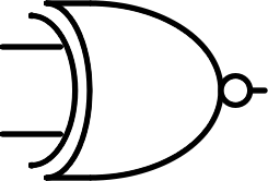 |
Inverted exclusive or | XNOR | $$\overline {A \oplus B}$$ |
Table 3 : useful binary two-inputs gates
In ternary logic, two-inputs gates are represented with a three by three matrix. Thus there are $$3^{3^3}=19683$$ possible such gates. Only six useful gates and their inverted versions will be de-scribed, however some other gates can be useful such as some asymmetrical gates (as in switching the inputs produces differ-ent results and the matrix is asymmetrical).
| Matrix | Schematic | Description | Name | Symbol |
|---|---|---|---|---|
| $$ \begin{bmatrix} - & - & - \\ - & 0 & 0\\ - & 0 & + \end{bmatrix} $$ | 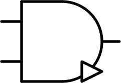 |
And / minimum | AND | $$A \times B$$ |
| $$ \begin{bmatrix} + & + & + \\ + & 0 & 0\\ + & 0 & - \end{bmatrix} $$ | 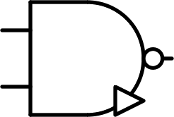 |
Inverted and / minimum | AND | $$\overline {A \times B}$$ |
| $$ \begin{bmatrix} - & 0 & + \\ 0 & 0 & +\\ + & + & + \end{bmatrix} $$ |  |
Or / maximum | OR | $$A + B$$ |
| $$ \begin{bmatrix} + & 0 & - \\ 0 & 0 & -\\ - & - & - \end{bmatrix} $$ |  |
Inverted or / maximum | NOR | $$\overline {A + B}$$ |
| $$ \begin{bmatrix} - & 0 & 0 \\ 0 & 0 & 0\\ 0 & 0 & + \end{bmatrix} $$ |  |
Consensus | CONS | $$A ⊠ B$$ |
| $$ \begin{bmatrix} + & 0 & 0 \\ 0 & 0 & 0\\ 0 & 0 & - \end{bmatrix} $$ | 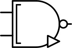 |
Inverted consensus | NCONS | $$\overline {A ⊠ B}$$ |
| $$ \begin{bmatrix} - & - & 0 \\ - & 0 & +\\ 0 & + & + \end{bmatrix} $$ |  |
Any | ANY | $$A ⊞ B$$ |
| $$ \begin{bmatrix} + & + & 0 \\ + & 0 & -\\ 0 & - & - \end{bmatrix} $$ |  |
Inverted any | NANY | $$\overline {A ⊞ B}$$ |
| $$ \begin{bmatrix} + & 0 & - \\ 0 & 0 & 0\\ - & 0 & + \end{bmatrix} $$ |  |
Multiplication | MUL | $$A \otimes B$$ |
| $$ \begin{bmatrix} - & 0 & + \\ 0 & 0 & 0\\ + & 0 & - \end{bmatrix} $$ |  |
Inverted multiplication | NMUL | $$\overline {A \otimes B}$$ |
| $$ \begin{bmatrix} + & - & 0 \\ - & 0 & +\\ 0 & + & - \end{bmatrix} $$ |  |
Addition | SUM | $$A \oplus B$$ |
| $$ \begin{bmatrix} - & + & 0 \\ + & 0 & -\\ 0 & - & + \end{bmatrix} $$ |  |
Inverted addition | NSUM | $$\overline {A \oplus B}$$ |
Table 4 : useful ternary two-inputs gates
AND and OR ternary gates are sometimes called MIN and MAX for obvious reasons. The MUL gate is also sometimes called XOR.
The gate symbols used here are similar to the US binary gate symbols with modifications for the more complex operations. In addition, as with the US symbols, a dot on the output signifies an inverted output. The small triangle indicates that it's a ternary gate, to differentiate between equivalent binary and ternary gates. The symbols are based on the binary AND and OR gates : if we only look at the 2×2 submatrix for zero and positive inputs of the ternary gates, some look like binary AND and other like binary OR, so this is the base used for their symbols, then alterations are added.
Formulae
Some gates are easy to implement with few transistors and resistors, while others require combining other simpler gates. This increases the cost but also the transmission time of the signal through the gate and thus the length of the transient before reaching the static phase with the correct output of the circuit. This can be a bottleneck for the frequency of a logic circuit such as a processor. Therefore, finding the best implementation of a gate is critical.
To find the formulas of logic gates from simple ones, I Python script is used to test every possible combinations of basic logic gates with simple operation prototypes. For instance, every combination with the pattern $$A \bigstar B$$ with $$\bigstar$$ a two-inputs gate. The script searches all the combinations for the simplest solutions with the smallest transistor and resistor cost.
As will be explained when looking at the CMOS implementation of those gates, the simple one-input gates are BUF, NOT, NNOT, PNOT as well as CLU and CLD if we allow the use of diodes. The simple two-inputs gates are NAND, NOR, NCONS and NANY.
As with binary algebra, many formulae help implementing the more complex gates. Some of the formulae are only useful be-cause they correspond to the CMOS implementations covered later.
| $$\overline{\overline{A}}=A$$ | $$|A| = \overline { \overline{A} \times A}$$ |
| $$A^{=-}=\check{A}$$ | $$\left \lceil{A}\right \rceil = A + (0)$$ |
| $$A^{=+}=\overline{\hat{A}}$$ | $$\left \lfloor{A}\right \rfloor = A \times (0)$$ |
| $$A$$╯╯$$=A$$╮ | $$\overline{A \times B}=\overline{A} + \overline{B}$$ |
| $$A$$╮╮$$=A$$╯ | $$\overline{A + B}=\overline{A} \times \overline{B}$$ |
| $$A^+ = A⊞(+)$$ | $$\overline{A⊠B}=\overline{A}⊠\overline{B}$$ |
| $$A^- = A⊞(-)$$ | $$\overline{A⊞B}=\overline{A}⊞\overline{B}$$ |
| $$A$$╯$$ = A \oplus (+)$$ | $$A \otimes B=\overline{A} \otimes \overline{B}$$ |
| $$A$$╮$$ = A \oplus (-)$$ | $$\overline{A \oplus B}=\overline{A} \oplus \overline{B}$$ |
| $$\overline{A \otimes B}=\overline{A} \otimes B=A \otimes \overline{B}$$ |
| $$A$$╯╮ $$=A$$╮╯$$=A$$╮╮╮$$=A$$╯╯╯$$=A$$ |
| $$A \otimes B = (A + \overline{B}) \times (\overline{A} + B) $$ |
| $$A \otimes B = \overline{ \overline{A \times B} \times A + B } $$ |
| $$\overline{A \otimes B} = \overline{ \overline{A + B} + A \times B } $$ |
| $$A \oplus B = \left( A⊞B ⊞ \overline {A⊠B} \right) ⊞ \overline {A⊠B}$$ |
| $$A \oplus B = \overline{ \overline{ A⊞B ⊞ \overline {A⊠B} } ⊞ A⊠B }$$ |
| $$(A \times B) ⊠ (A+B) = A⊠B$$ |
Basic CMOS implementations
CMOS chip selection
In order to assess the feasibility of ternary processors, implementations of the basic ternary logic gates will be first be described. Current processors use Complementary Metal Oxide Semiconductor (CMOS) logic with both PMOS and MNOS. Without access to expensive micro-fabrication, CMOS circuits will be built using the CD4007 chip. This chip contains three CMOS pairs but only one is usable as they are not independent. This chip comes in a DIP14 package, very useful for tests on breadboard and for custom PCB with DIP sockets to change the chip if it breaks down.
This chip works with voltages up to $$15V$$ so an adjustable dual-rail power supply is used to test different configurations.
Fundamental gates
The ternary inverter actually comes in three versions, the neutral NOT and the positive and negatively biased NNOT and PNOT, but they don't require more circuitry : just a single CMOS pair. The other basic gates have two inputs, thus two CMOS pairs. For the two-input gates, the two corresponding transistors of the two CMOS pairs can either be setup in parallel or in series. Two configurations for the NMOS and the PMOS, so four configurations in total for the two pairs. Those are the four basic gates : NAND, NOR, NCONS, NANY [6][7].
Note that the non-inverted two-inputs gates requires an additional regular inverter on the output of the simpler inverted versions.
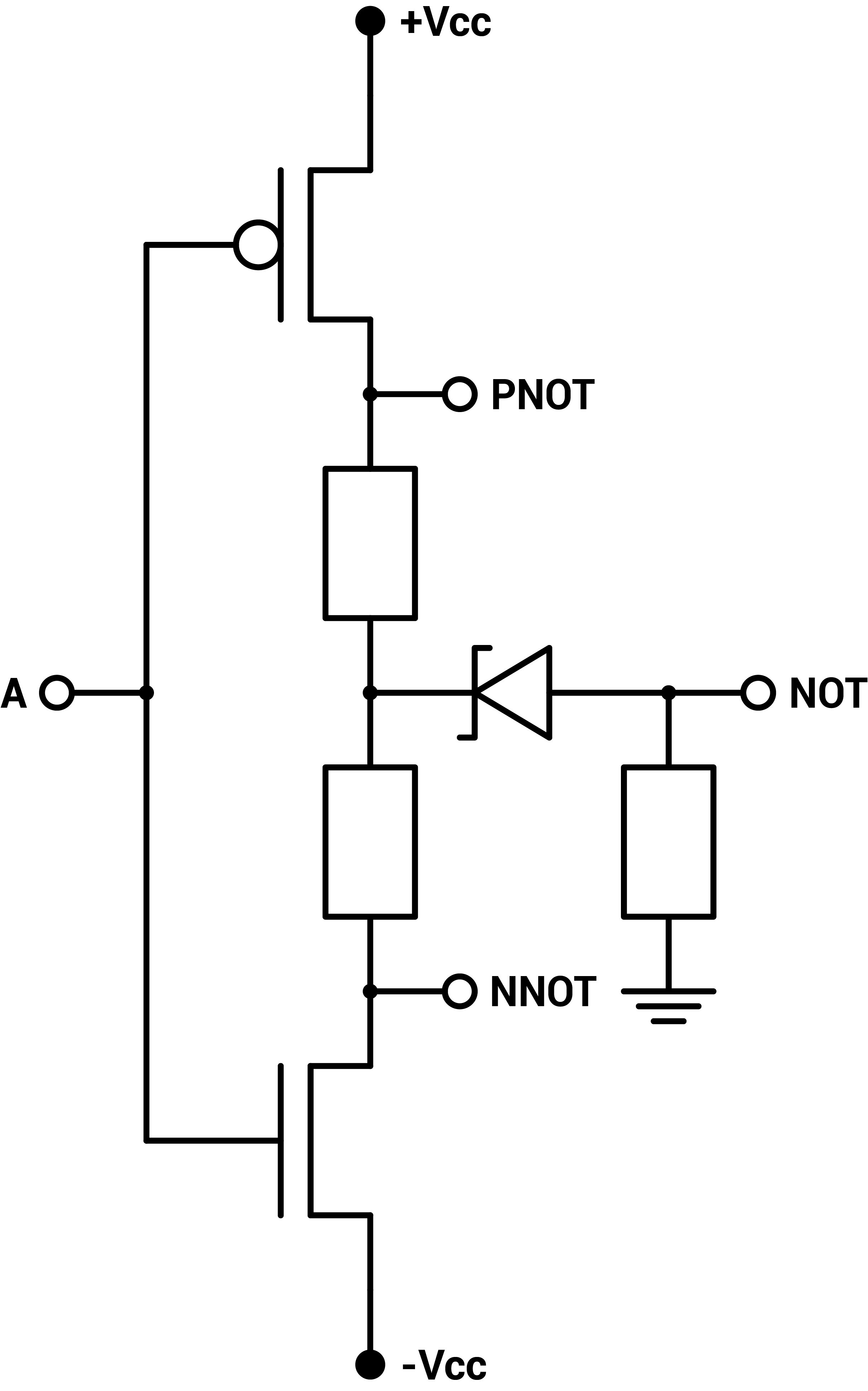
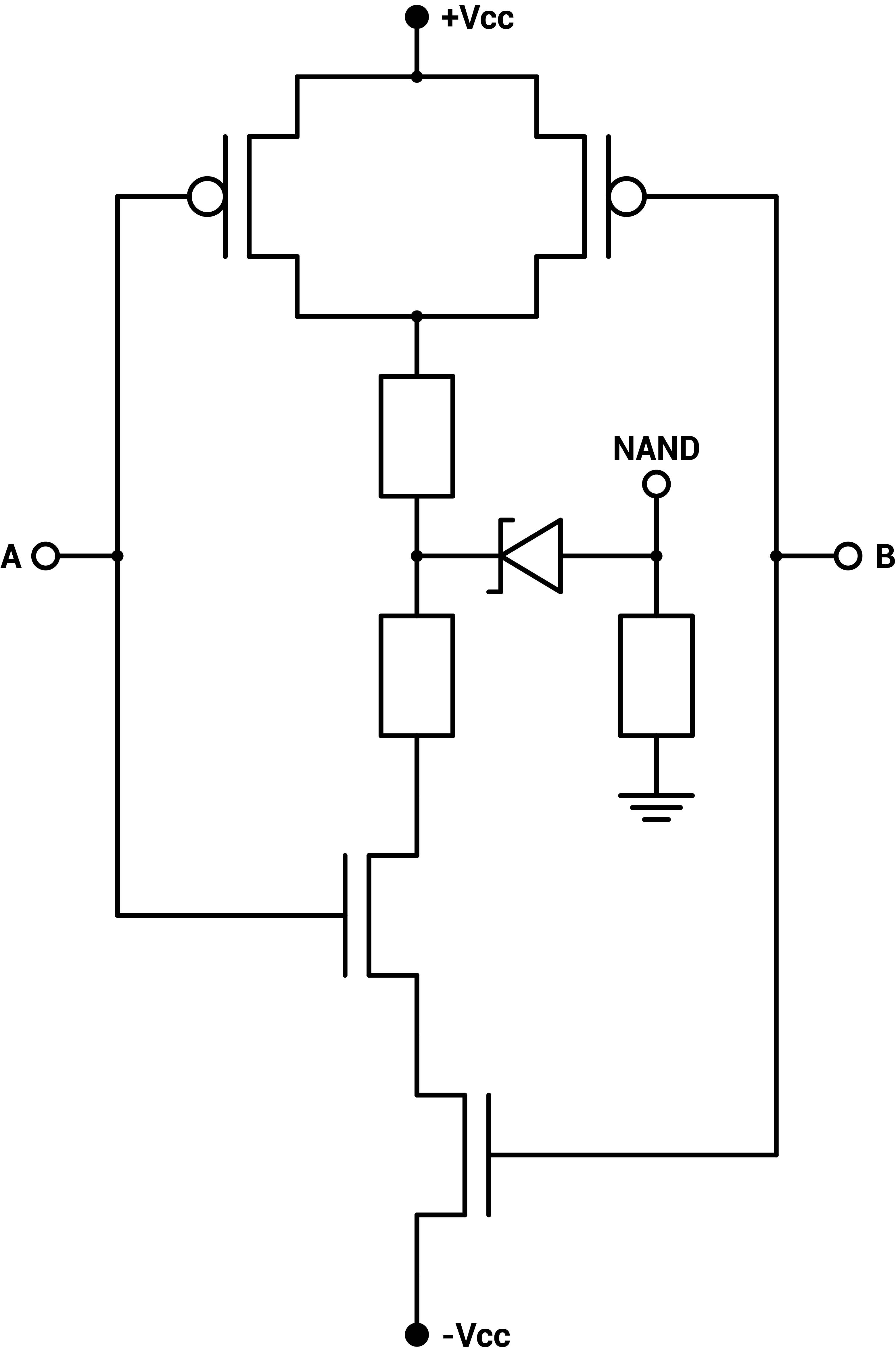
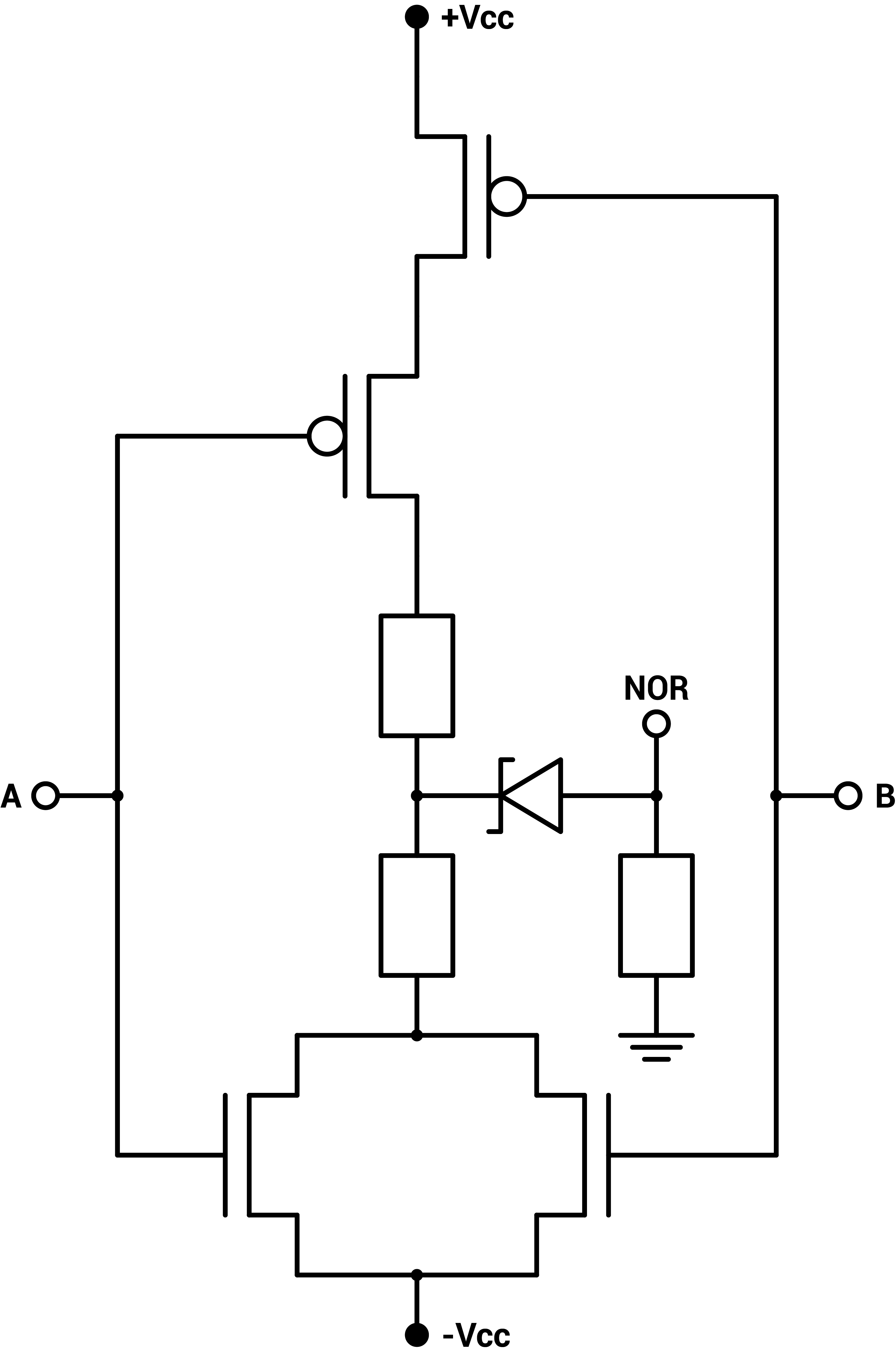
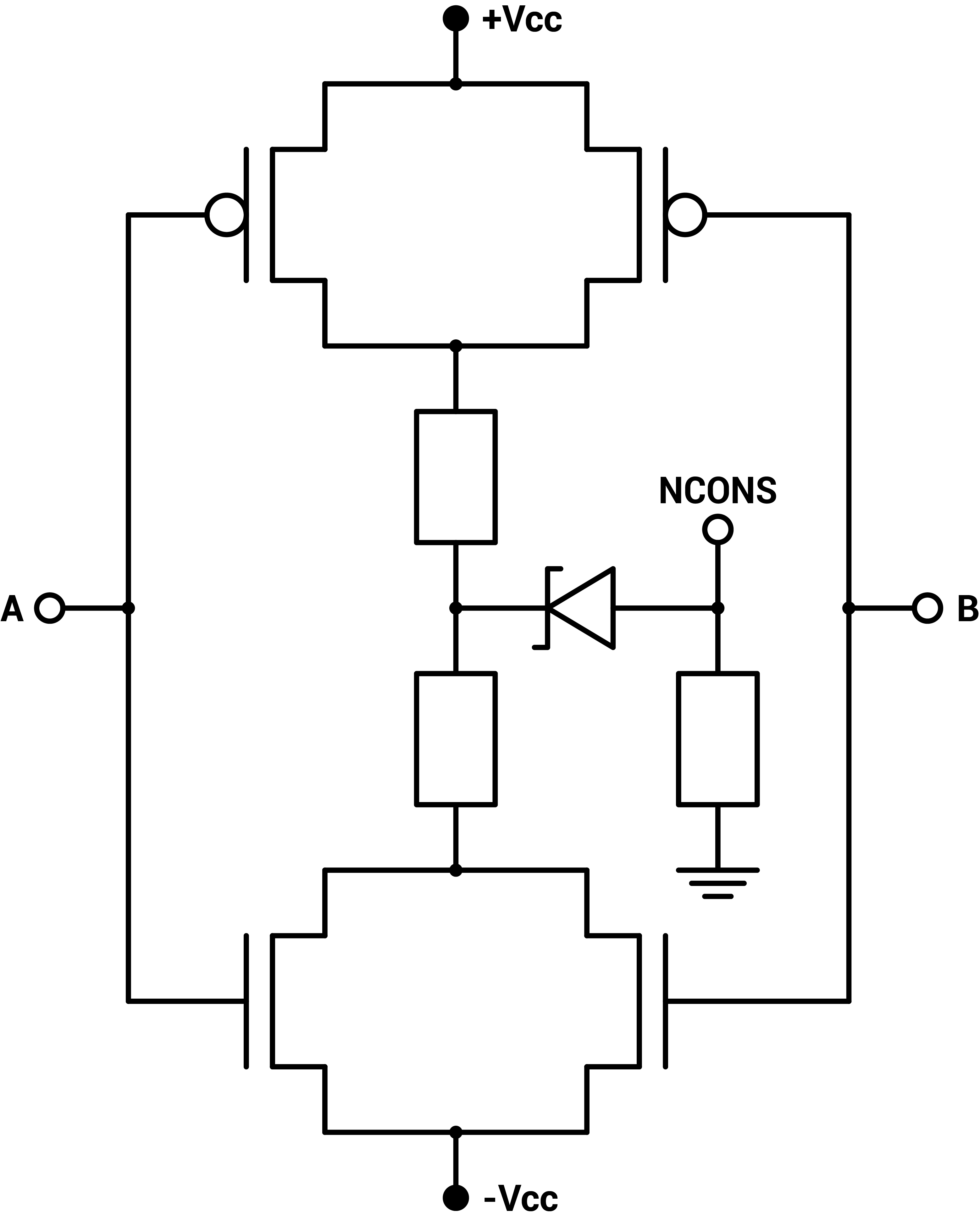
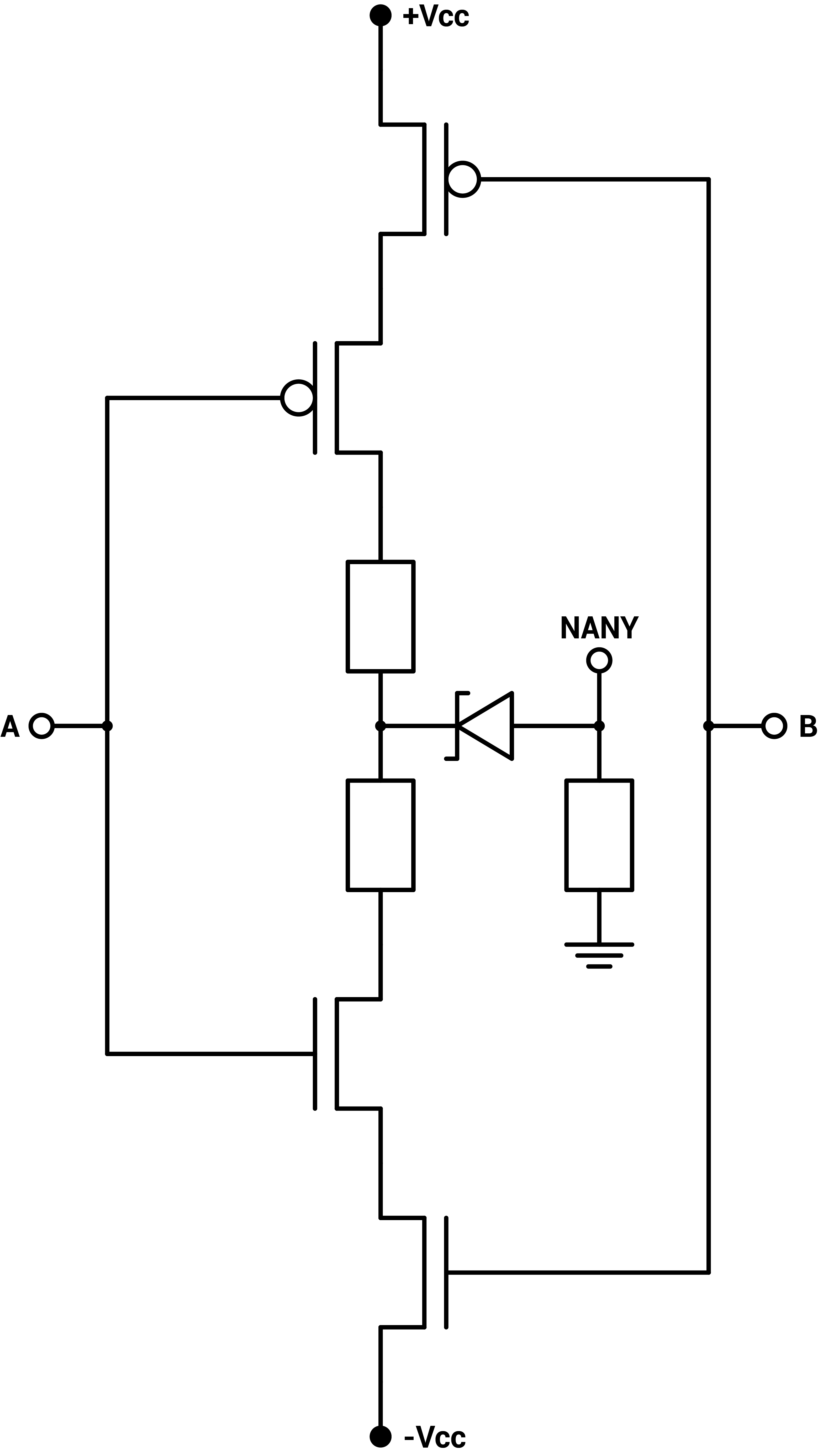
Figure 1 : Zener-CMOS implementation of ternary inverters, ternary NAND, ternary NOR, ternary NCONS and ternary NANY
The CD4007 CMOS pair has a small negative voltage bias so the power supply is set to $$-5V$$ $$+5.7V$$. Two $$1kΩ$$ resistors are used between the PMOS and NMOS to stabilize the output. Additionally, a voltage shifter using a small $$2.2V$$ Zener diode and a $$100kΩ$$ pull-down resistor to ground are used to create a flat and neutral zero state. Without the voltage shifter, the neutral state corresponding to a 0 is on a slope, making it unstable when using the output to drive another gate, as can be seen on figure 2.

Figure 2 : CMOS ternary inverter input/output characteristics
Multiplication gate
The more complex multiplication gate requires the combination of the fundamental gates described above, following the formula listed previously.
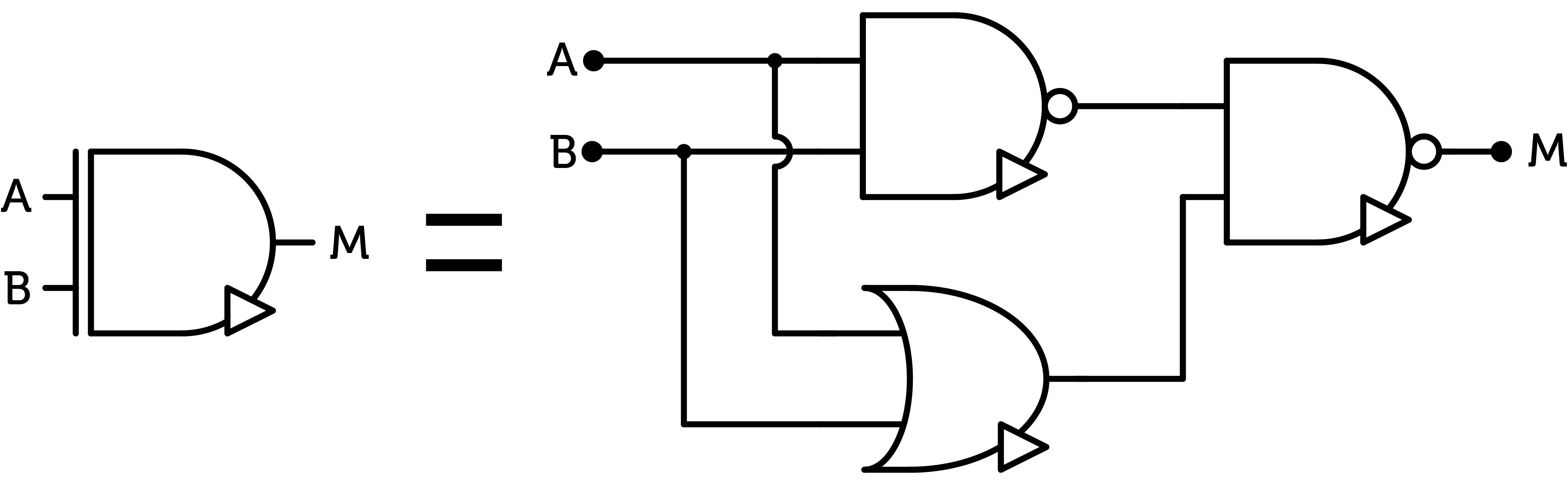
Figure 3 : multiplication gate equivalent circuit
This equivalent circuit uses $$7$$ CMOS pairs when implementing each gate separately. Some transistors can be factorized to reduce the cost of this gate ; however, this requires transistor-level control of the circuit which is not possible using the CD4007 chip. Therefore, this will not be explored in this paper.
The inverted multiplication gate can be built using the same number of transistors, which can be useful in certain circuits.
Addition gate
The addition gate is a critical component for ALU circuits so a working cheap implementation is a major issue. As with the multiplication gate, the sum gate can be implemented using the fundamental gates.
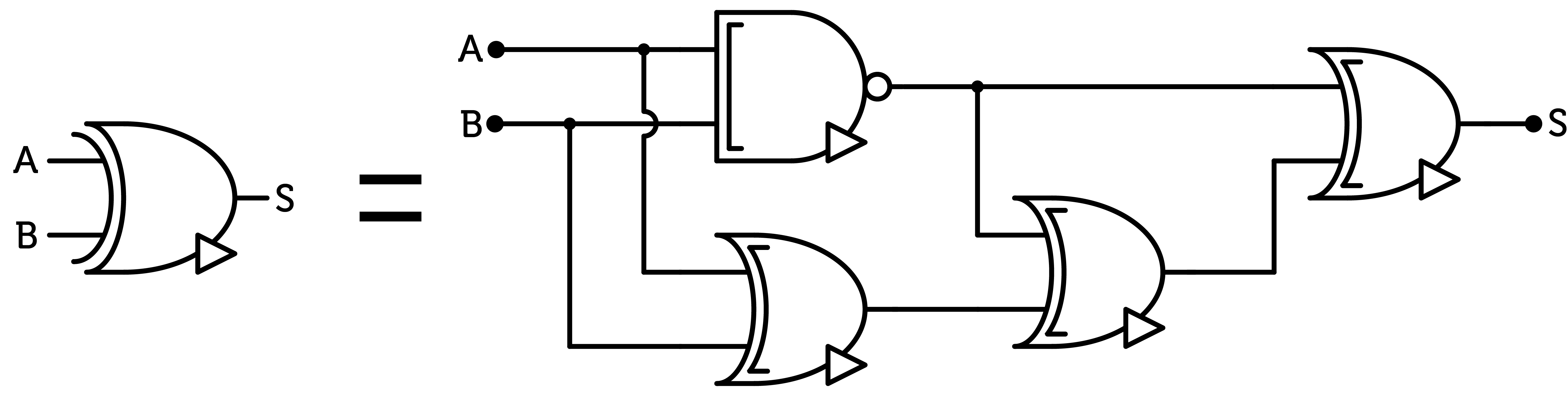
Figure 4 : sum gate equivalent circuit
This equivalent circuit uses $$11$$ CMOS pairs. However, the inverted version of the sum gate is cheaper as it uses one less inverter, thus one less CMOS pair. Again, some transistors can be factorized to reduce the cost of this gate.
Ternary ALU design
Basic design
The main operation of the Arithmetic Logic Unit is the addition. This operation, as in any numerical base requires a carry system, a way to propagate the carry from the addition from one digit to the next. For the sake of simplicity, a ripple-carry system will be used in this design and not a carry-lookahead. That means adding the two trits of one digit of the words requires the carry of the previous pair of digits, therefore we have to wait for the previous sum to be completed. Consequently, as the word length increases, so does the time required for the operation to complete in a linear way. In a full processor, this reduces the maximum frequency, or requires complex timing and scheduling.
As with binary, we start by creating a half-adder, which add two trits and outputs the sum as well as the carry of this operation. The matrices of the sum and carry of two trits are given in figure 5. We recognize the sum of A and B to be the SUM gate and the carry is the CONS gate.
Figure 5 : sum of two trits (left) and carry of two trits (right)
Thus, a ternary half-adder can easily be built.
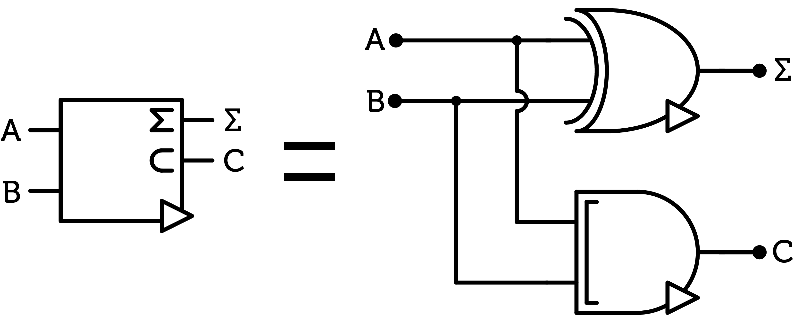
Figure 6 : ternary half-adder
Then two half-adders are combined to create a full-adder to add two trits as well as the previous carry. The carries of the two additions also have to be combined with an ANY gate.
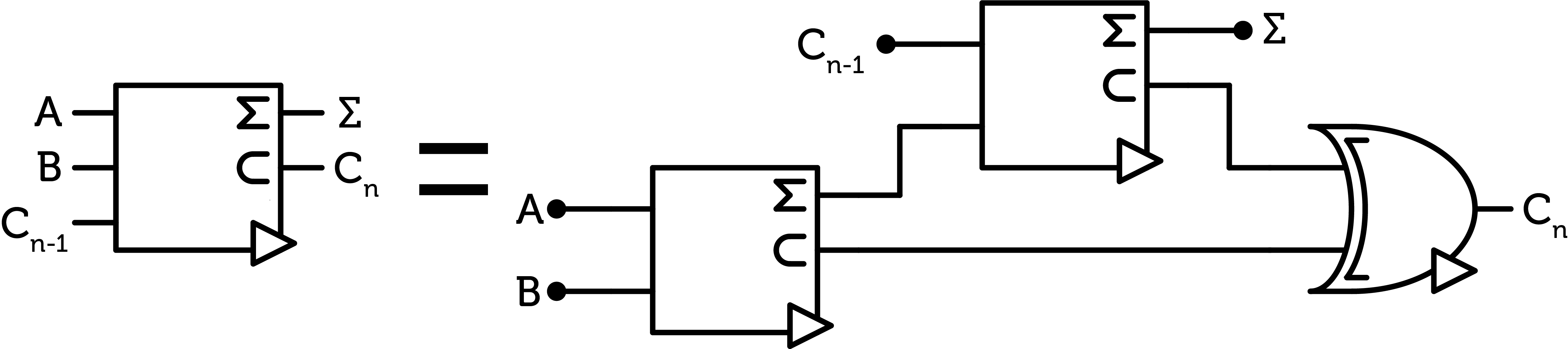
Figure 7 : ternary full-adder
This is the heart of the ALU. The first and last additions of the chain of digits are special as they respectively don’t have a previous carry and don’t have to output a carry. Therefore, the first digit only requires one half-adder, and the last one requires two SUM gates.
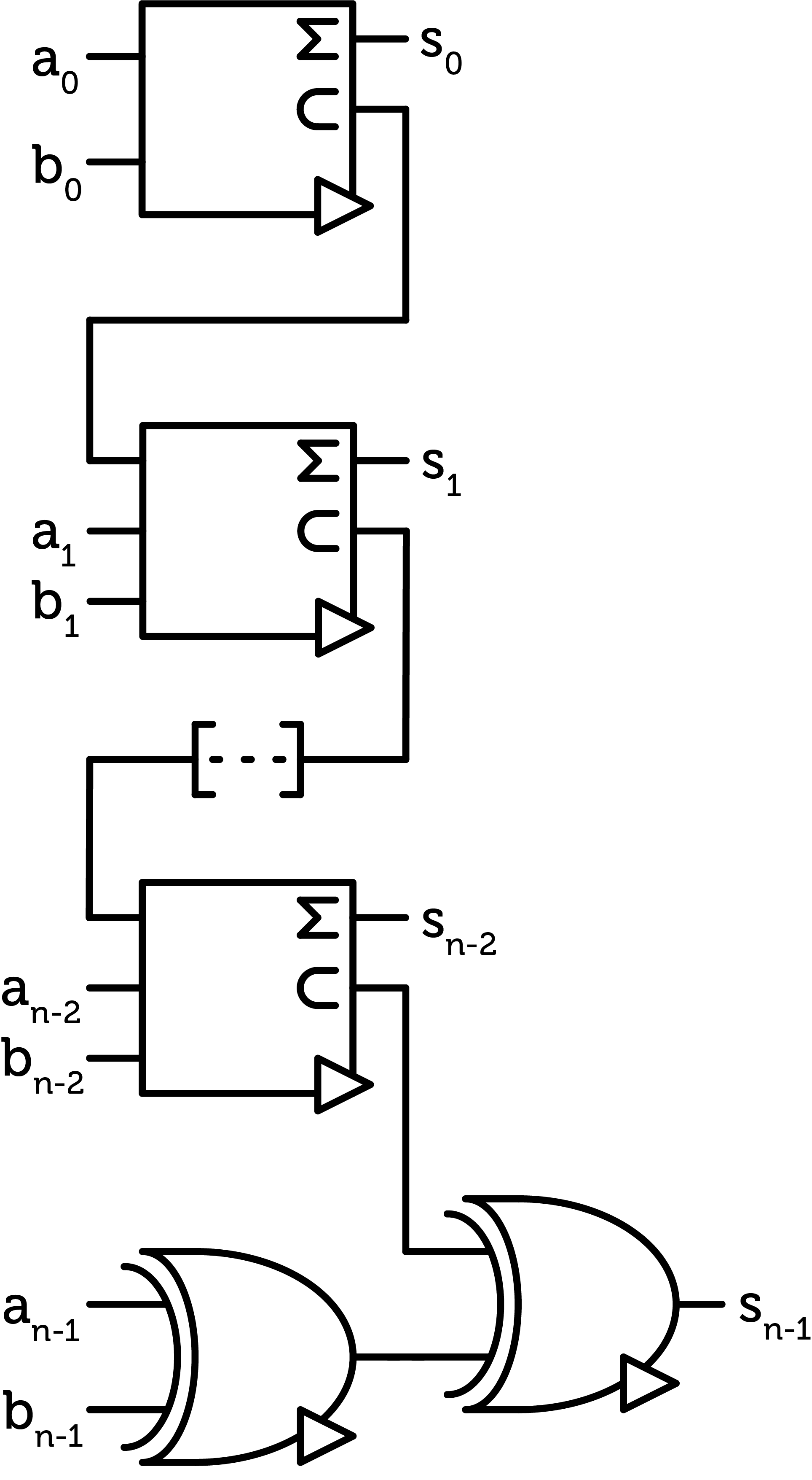
Figure 8 : ternary ALU chain
Some ALU also include a flag signal for the overflow (when the operation results in a number outside the range of the architecture). It can be achieved by replacing the circuitry of the last digit with a usual full-adder. This of course increases the cost.
Subtraction
As explained earlier, balanced ternary logic allows easy operations using positive and negative numbers. To negate a ternary number, the only process is to inverter every trit. This, an ALU that does only addition can do subtraction by negating one of the inputs.
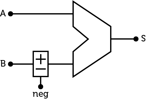
Figure 9 : ALU with negating circuit
A simple circuit to negate a ternary word uses multiplication gates. Each trit of the word is fed in a multiplication gate and a common signal is used to control the sign of the output word.
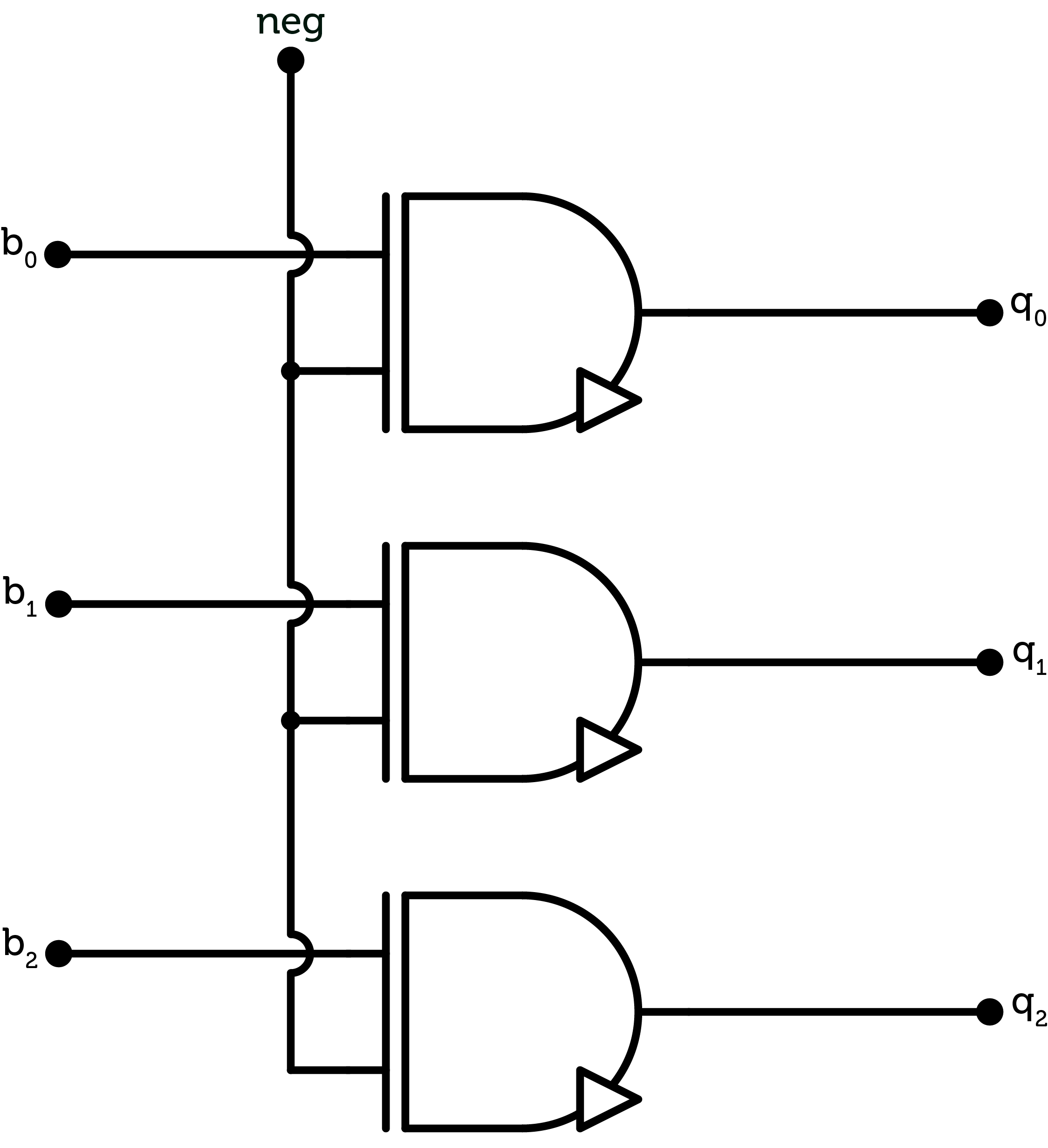
Figure 10 : negating circuit
Optimization
The number of CMOS pairs used for the ALU circuit can be reduced. Only the addition circuit will be considered here.
First, the fundamental gate of the ALU is the SUM gate. The SUM gate costs $$11$$ CMOS pairs. Then to build a half-adder, a SUM gate and a CONS gate are needed for a total of $$14$$ CMOS pairs. Then the full-adder requires two half-adders and an ANY gate, $$31$$ CMOS pairs. The first digit of the ALU is a single half adder (because there is no incoming carry trit), $$14$$ CMOS pairs, and the last digits is two SUM gates (no output carry trit, even though it is often the case that the last carry bit in a binary ALU is stored in a flag for branching instructions and the ability to do calculations with multiple words), $$22$$ CMOS pairs ; the rest are full-adders. For a n-trit ALU ($$n≥2$$), the total cost of the ALU (not including the sign controller required for subtraction) is $$31n-26$$ CMOS pairs. For a 3-trit ALU, that amounts to $$67$$ CMOS pairs.
We can spare one CONS gate per half-adder by using the NCONS gate in the SUM gate and adding a NOT gate. That saves $$2$$ CMOS pairs per half-adder. The new total cost is $$27n-20$$ CMOS pairs, $$61$$ CMOS pairs for a 3-trit ALU.
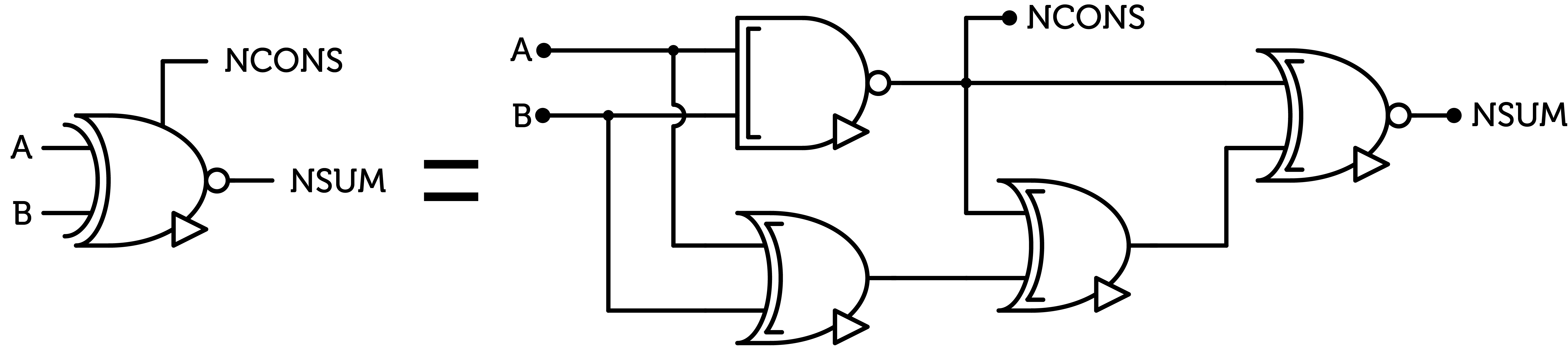
Figure 11 : ternary full-adder
Another economy comes from the formulae listed previously. If we invert both inputs of a SUM gate, the output is unchanged.
$$A⊞B=\overline{A}⊞\overline{B}$$
$$A \otimes B=\overline{A} \otimes \overline{B}$$
$$A \oplus B=\overline{A} \oplus \overline{B}$$
The trick is to use inverted gates before the input, and since those inverted gates are usually cheaper, we can save transistors. This is simpler to understand with diagrams.
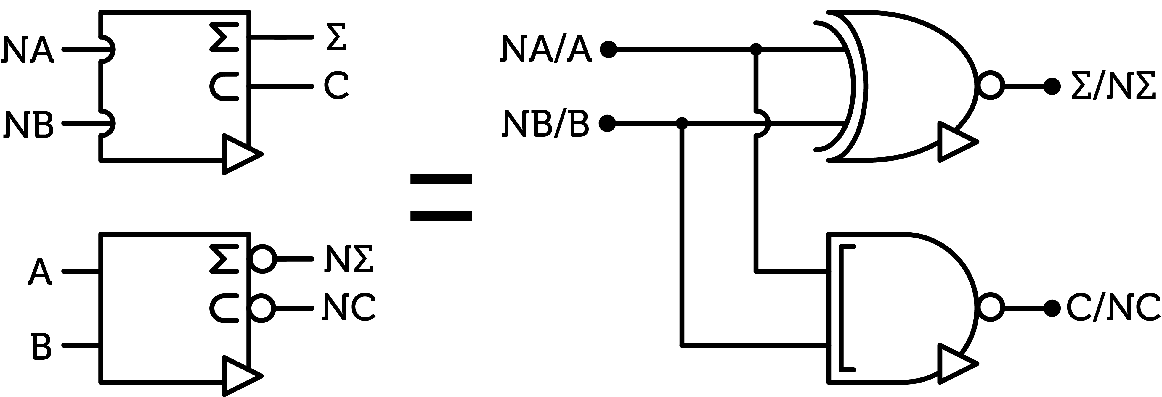
Figure 12 : N-half-adder
Here is an alternative half-adder. Two symbols are used and here is why. The circle on the output still means that the output is inverted compared to the default gate (here the half-adder). The round cup on the input is supposed to indicate an inverter should be present on the input ; that is, to get the behaviour of the default gate, we have to invert this input. Here, the two symbols, taken with the labels, are the same : to get the behaviour of the default half-adder, we can either invert both output or both inputs. This is a direct consequence of the formulae listed above.
Using this N-half-adder, we can create a N-full-adder.
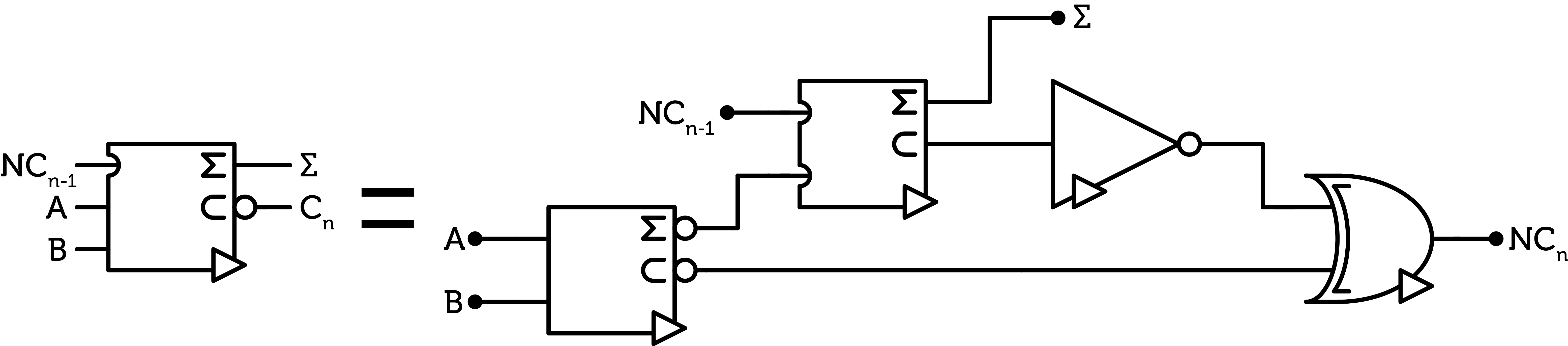
Figure 13 : N-full-adder
Again, both N-half-adders on this diagram correspond to the same internal circuitry described above. However, on the bottom one, we feed the original A and B signals, so we get the inverted sum and inverted carry of A and B. While on the top one, we feed in the inverted incoming carry and the inverted sum from the first N-half-adder, so we get the un-inverted final sum and the uninverted carry. So, one carry is inverted and the other is not. To combine the two carries, we have to invert one and thus add a NOT gate. Then, to get the inverted total carry, a NANY is used, which is more expensive than the ANY gate.
Finally, the full ALU can be built again. As expected, the first and last digits are also different.
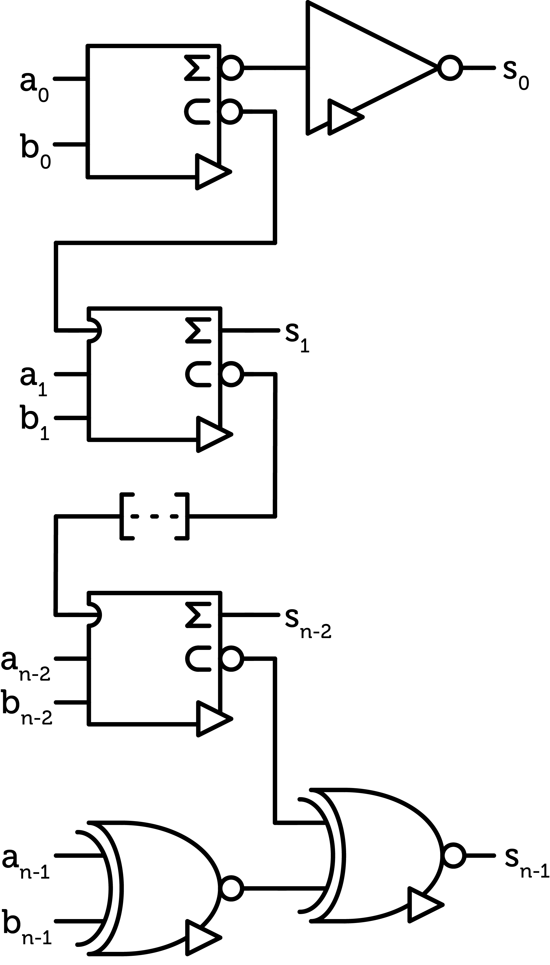
Figure 14 : new adder chain
With those modifications, the N-half-adder costs 10 CMOS pairs, the N-full-adder 24 CMOS pairs, the first digit 11 CMOS pairs and the last digit $$21$$ CMOS pairs. The total and final cost after optimization is $$24n-16$$ CMOS pairs, 56 for the 3-trit ALU.
Beside an economy of transistors, the optimizations also reduce the number of CMOS pairs the signal has to propagate through, and thus increases the maximum frequency of the processor. Calculating the critical path that will be explained later, a n-trit ternary ALU has a propagation delay of $$9n-7$$ CMOS propagation delays.
Further economy could be possible at the transistor level instead of pairs of transistors using the CD4007 chips as a reference.
Physical build of the ALU
Sourcing materials
The CD4007 chips were bought on ic-online.com. The custom PCBs were designed on EasyEDA and manufactured by JLCPCB. All other electrical components were bought from various suppliers on Aliexpress and eBay.
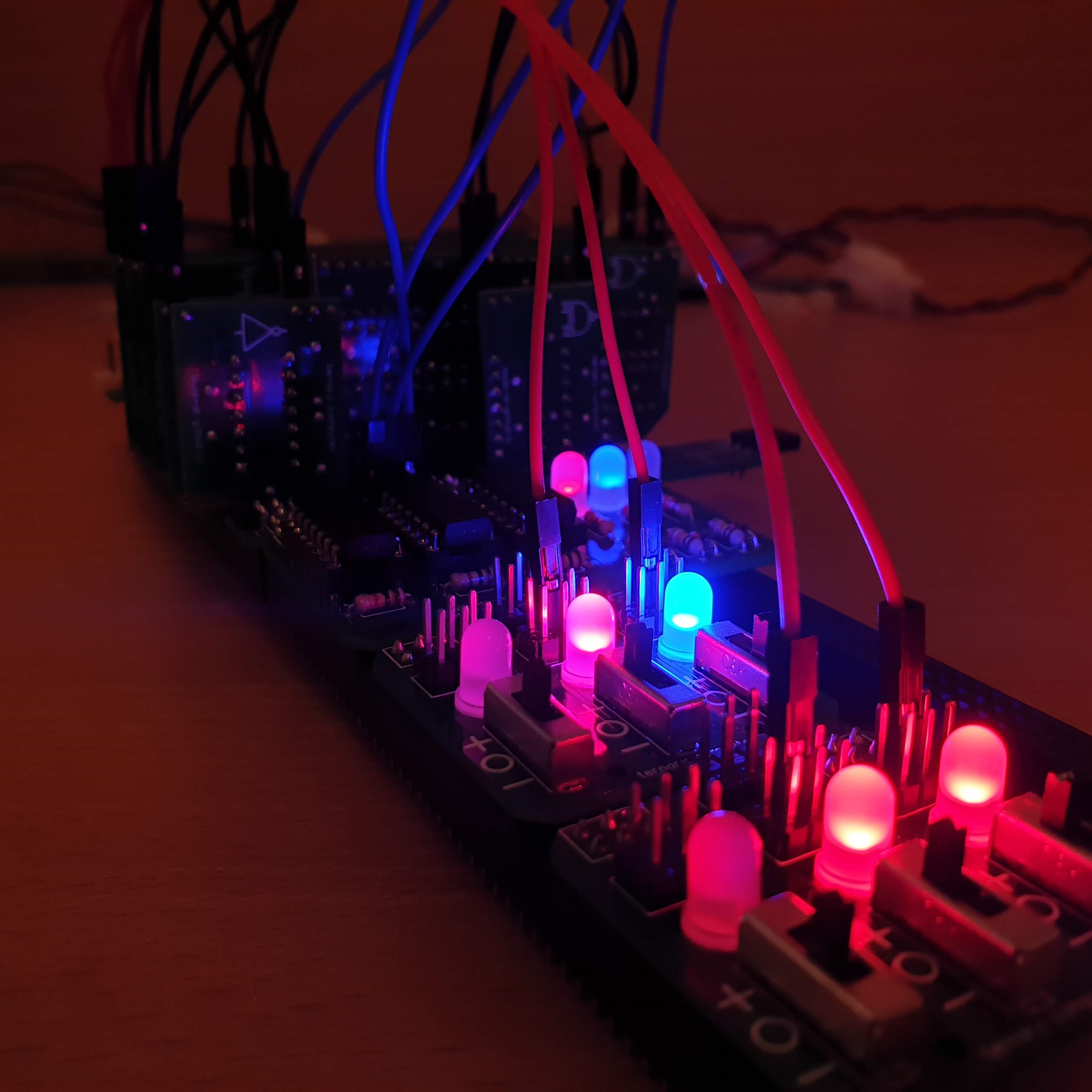
Ternary 2-trit ALU
In order to verify the feasibility of ternary logic circuits using CMOS pairs, a 2-trit ALU with subtraction ability has been built. It uses almost all the gates described above including the SUM and MUL gates.
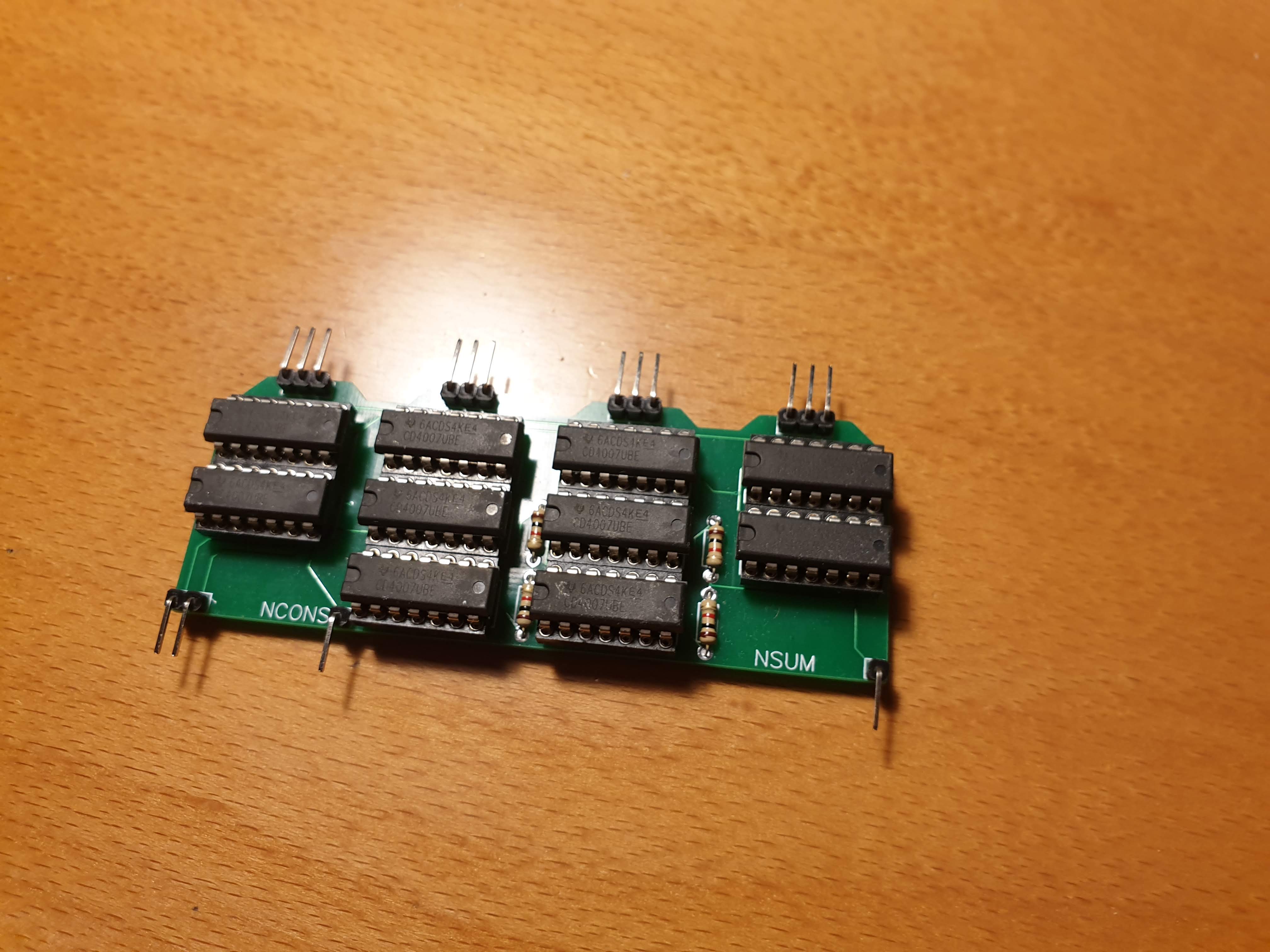
Figure 15 : PCB of the ternary SUM gate using CD4007 chips
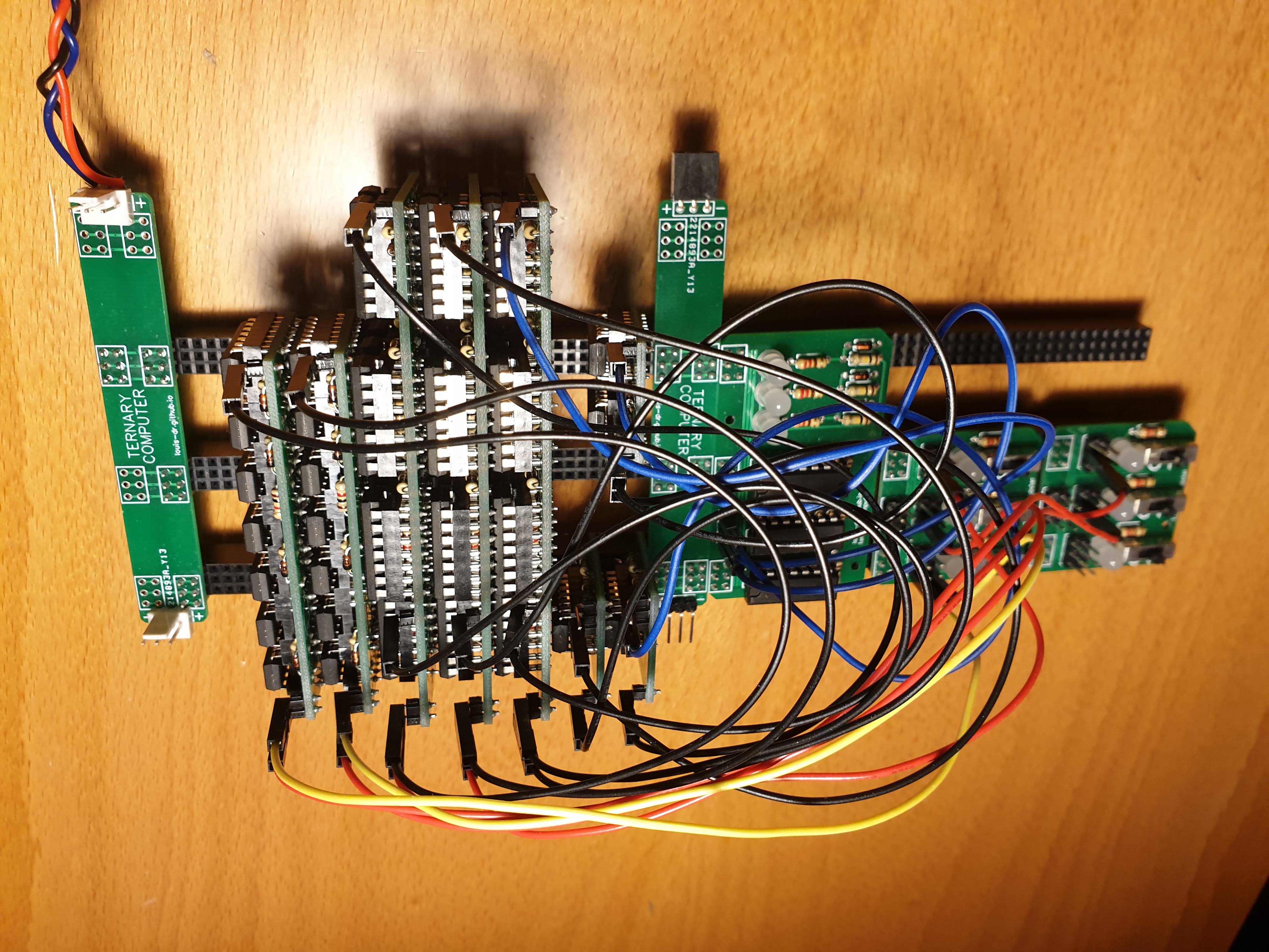
Figure 16 : full circuit of the working 2-trit ALU
A more in-depth description of the design and testing process as well as a demonstration of the circuit in action can be found in the other articles on this website.
Comparison with binary
Metrics
Performance of processors can be measured on power consumption, maximal frequency and cost. Only the latter two will be compared here.
Maximal frequency is determined by the longest path of the electric signal in the circuit, the critical path. The time the signal takes to propagate through the circuit can depend on multiple factors, but only the propagation time of the CMOS transistors will be considered. The comparison will be measured using the number of propagation delays of the critical path of the circuit. One CMOS propagation delay will refer to one propagation delay of the CMOS pair (about 20ns for the CD4007 for example). Simple gates such as NOT, NAND, NOR, NCONS and NANY only require a single CMOS propagation delay, but the more complex MUL, SUM and NSUM gates require respectively $$3$$, $$6$$ and $$5$$ CMOS propagation delays.
Cost itself can be broken down on multiple factors. Processor fabrication costs are increased by the technology used, area of the die, number of fabrication steps, etc. In the case of ternary circuits, the technology is not explored in this report as it would require extensive experimenting using micro-fabrication. The number of transistors affect directly the area of semiconductor necessary. The number of fabrication steps depends in part on the technology used, and the density of interconnections between transistors requiring more or less layers on top of the semiconductor. For the sake of simplicity and to get a first idea of a comparison, the cost will be modelled by the number of CMOS pairs necessary.
Binary ALU design
The ternary ALU described above will be compared to a binary ALU using a similar design, that is a n-bit ALU with a ripple carry system.
Using similar CMOS architecture, the binary inverter (NOT) costs a single CMOS pair, and the binary NAND and NOR two-inputs gates cost two CMOS pairs each. All three of those gates require a single CMOS propagation delay
The equivalent of the SUM gate of the ternary ALU in binary is the XOR gate. If we were to implement this gate as a combination of simpler gates (binary NAND and NOR) as we did for the ternary SUM gate, we can use the following formula.
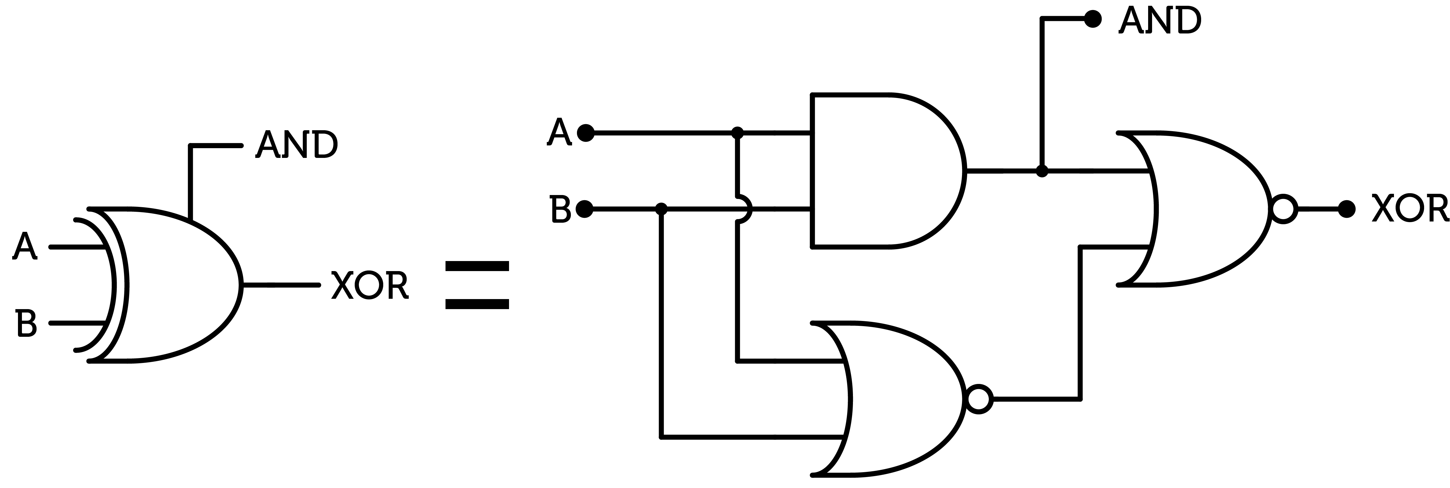
Figure 17 : binary XOR gate
This brings the cost of this gate to $$8$$ CMOS pairs. Using binary algebra formulae, we can deduce that the cost for the XNOR gate is the same. The propagation delay is of $$3$$ CMOS propagation delays.
The binary half-adder is built with a XOR gate for the sum and a AND gate for the carry. The AND gate inside the COR gate can be used to spare some transistors. Two half-adders are used to build the full-adder and an OR gate combines the two carries.
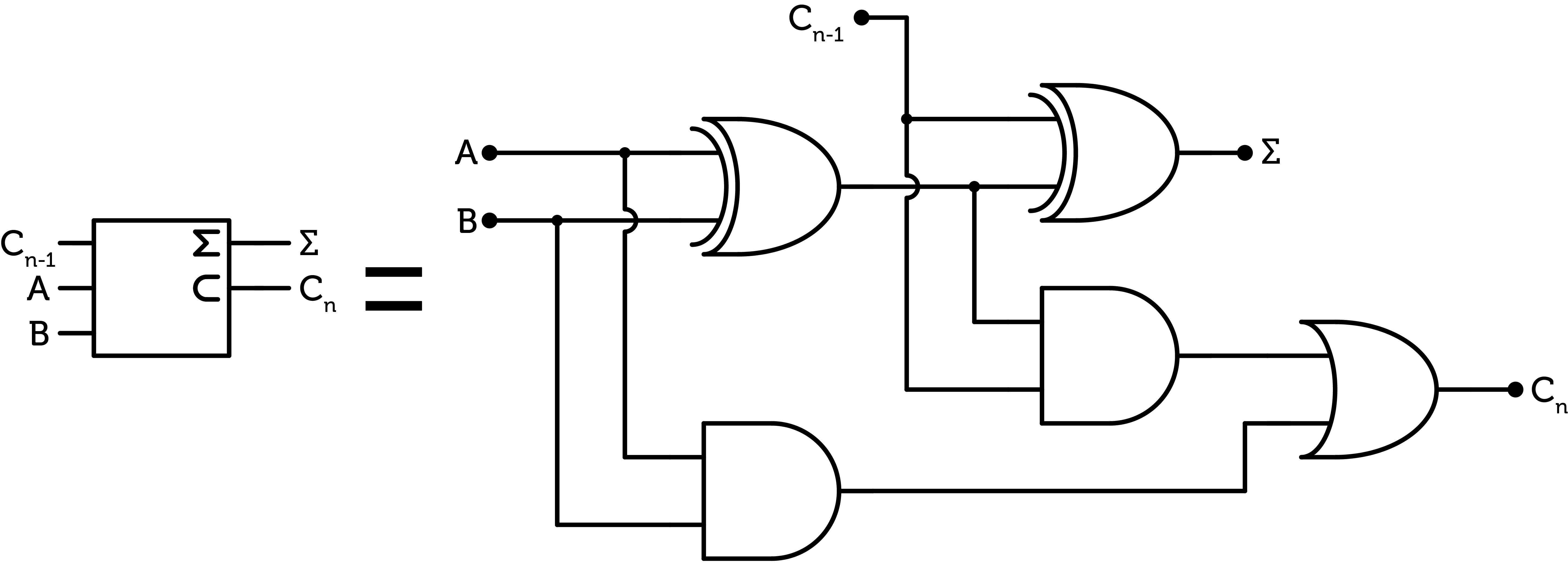
Figure 18 : binary full-adder
This full-adder costs $$19$$ CMOS pairs and has a propagation delay of $$6$$ and $$7$$ CMOS propagation delays for the sum and the carry respectively. The first bit of the ALU only requires a single half-adder and the last one only two XOR gates using a similar architecture to the ternary ALU.
However, some processors use a different implementation of the XOR gate using Pass Transistor Logic [8], where the transistors are not connected to the power supply or ground, but to other gate outputs. This other logic family allows substantial cost reductions but also require more testing as the output of a PTL gate is not directly connected to the power supply but has to be able to drive other gates in the circuit. This can require additional circuitry. There exist many different PTL-like technologies such as Double-Pass Transistor Logic, Swing Restored Pass Transistor Logic and Complementary Pass Transistor Logic. They will not be compared in this report. However, a common PTL CMOS XOR gate can be built using only $$6$$ transistors.
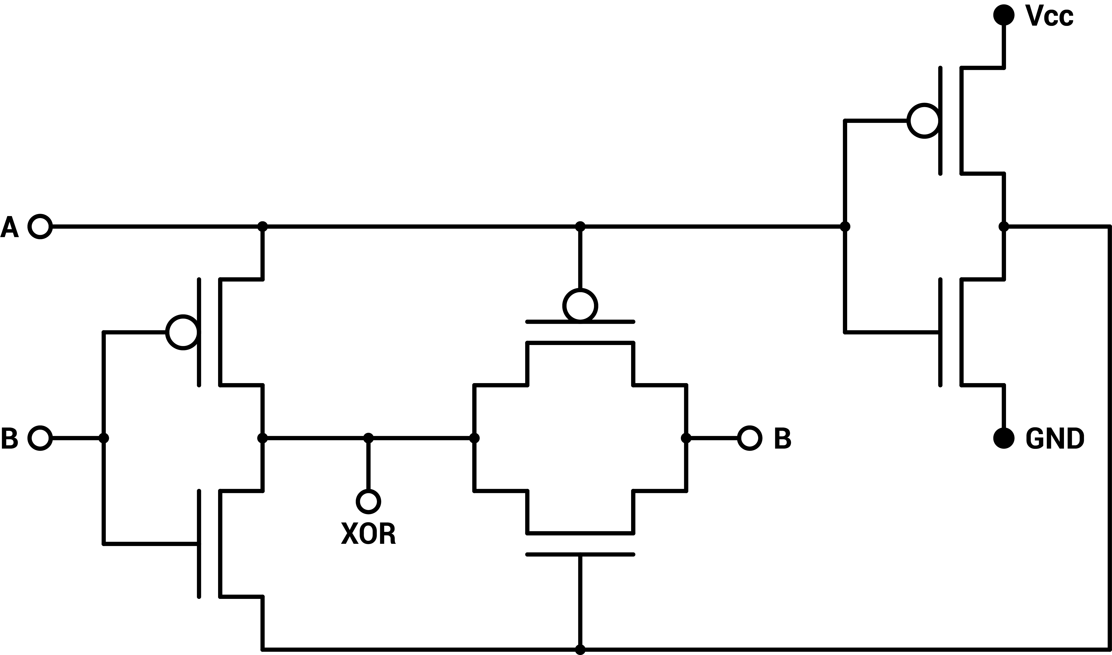
Figure 19 : PTL CMOS binary XOR gate
Thus, the cost of this XOR gate is only $$3$$ CMOS pairs, and the delay is $$2$$ CMOS propagation delays. As this XOR doesn’t contain a AND gate, we have to add it. However, we can use cheaper and faster NAND gates.
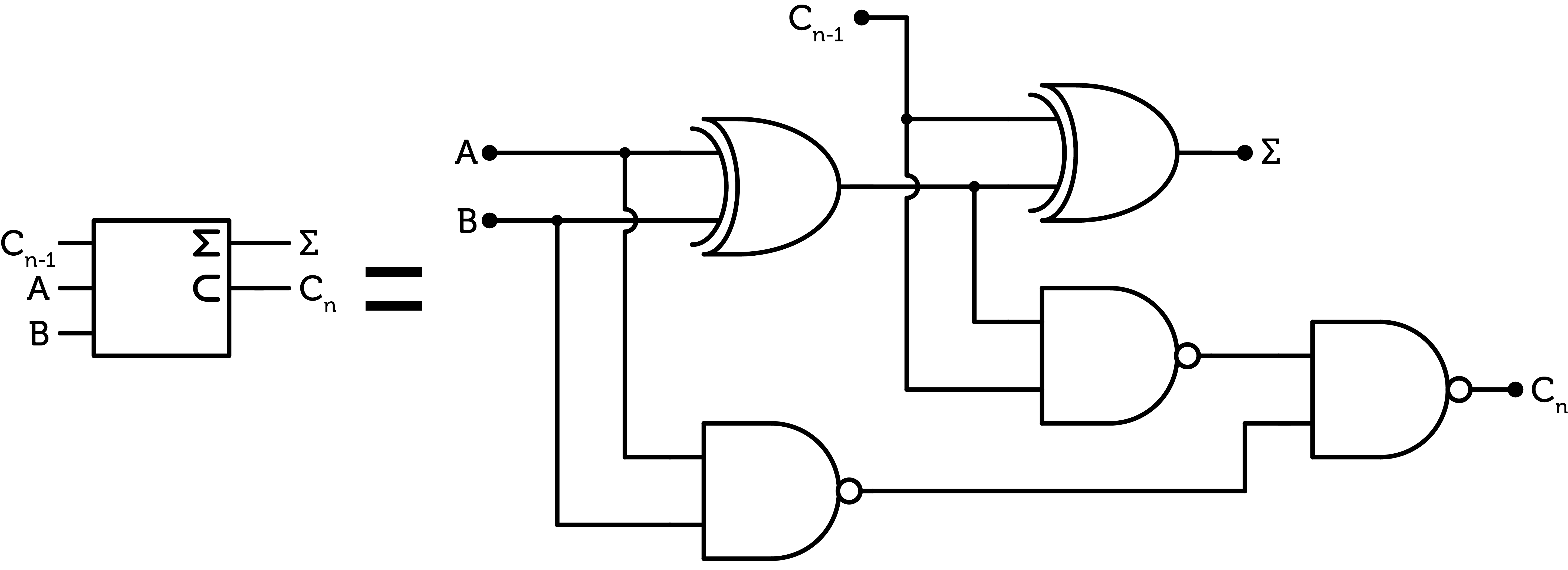
Figure 20 : alternative binary full-adder for the PTL XOR
This full-adder costs $$12$$ CMOS pairs and has a propagation delay of $$4$$ CMOS propagation delays for both the sum and the carry.
Both implementations will be considered in the comparison. Without PTL logic, a n-bit binary ALU (without the subtraction circuit) costs $$19n-14$$ CMOS pairs and has a propagation delay of $$7n-6$$ CMOS propagation delays. With PTL logic, a n-bit binary ALU costs $$12n-13$$ CMOS pairs and has a propagation delay of $$4n-3$$ CMOS propagation delays.
Results
Plotting the expected cost and propagation delay for different number of digits in the three different architectures as a function of the maximum range of values, we get the following results.

Figure 21 : cost comparison

Figure 22 : propagation delay comparison
As we can see, while the proposed ternary ALU is substantially cheaper and faster than a similar binary ALU for equal maximum range of values, using Pass Transistor Logic brings a considerable advantage to binary over balanced ternary.
Critical analysis
This comparison hints that ternary logic is not a worthwhile alternative to binary. However, binary logic has decades of advance in research, including PTL optimization. Using similar CMOS design, balanced ternary still presents an advantage over binary. Therefore, it can be expected that transistor-level design optimization applied to ternary logic can rival current binary processors.
Many assumptions have been made in this analysis. A more thorough analysis would require experimenting at the semiconductor level and take into account power consumption as well.
Moreover, this project only explores balanced ternary ALU. Unbalanced ternary logic might require less complex circuitry for some components of the processor such as look-ahead carry systems [9].
Conclusion
Balanced ternary logic can be computed on CMOS circuitry, as shown with the realization of the ternary ALU proposed in this report. It is overall cheaper and faster than similar basic binary logic, however, decades of research on transistor-level optimization allow binary to surpass the ternary logic presented.
More experimenting with other logic families such as Transistor Pass Logic should be carried out to try to match the performance of optimized binary circuits. Research on the realization of ternary circuits in integrated circuits is required to conclude more accurately on the potential gains of ternary logic and its uses. Unbalanced ternary logic should be explored and compared to balanced ternary logic.
References
[1] Stanley L. Hurst. 1984. Multiple-Valued Logic – its Status and its Future. IEEE Transactions on Computers. Vol. c-33, No. 12, December 1984.
[2] C.B. Tompkins, J.H. Wakelin, Engineering Research Associ-ates Inc. 1950. High-speed computing devices. McGraw-Hill Book Company Inc.
[3] N. Brusentsov, J.R. Alvarez. 2006. Ternary Computers : The Setun and the Setun 70. Soviet and Russian Computing. July 2006.
[4] W. Alexander. 1964. The Ternary Computer. Electronics and Power. Vol. 10, Issue 2, February 1964.
[5] Douglas W. Jones. 2012. Standard Ternary Logic. The Ter-nary Manifesto. www.cs.uiowa.edu/~jones/ternary.
[6] H.T. Mouftah. 1976. A Study on the Implementation of Three-Valued Logic. Proceedings of the sixth international sym-posium on multiple-valued logic, May 1976, 123-126.
[7] H.T. Mouftah. 1978. Ternary Logic Circuits with CMOS Integrated Circuits. US patent 4,107,549, Aug. 15, 1978.
[8] R.P. MeenaakshiSundari, R. Anita, M.K. Anandkumar. 2013. Implementation of Low Power CMOS Full Adders Using Pass Transistor Logic. IOSR Journal of VLSI and Signal Processing. Vol. 2, Issue 5 (May. – Jun. 2013).
[9] Douglas W. Jones. 2012. Fast Ternary Addition. The Ternary Manifesto. www.cs.uiowa.edu/~jones/ternary.
This article is part of my series of projects around Ternary Computing and Processor Design. Click here to see the list of projects of this series.
Go back to the list of projects