This article is part of my series of projects around Ternary Computing and Processor Design. Click here to see the list of projects of this series.
In this project, I implemented my first architecture in both binary and ternary logic using my TernaryVerilog hardware description language and tool suite.
Malvino's SAP1
The Simple-As-Possible 1 (SAP1) processor is a very basic architecture introduced by Albert Paul Malvino in his book Digital Computer Electronics to explain how processors and their most fundamental components work.

SAP1 block diagram
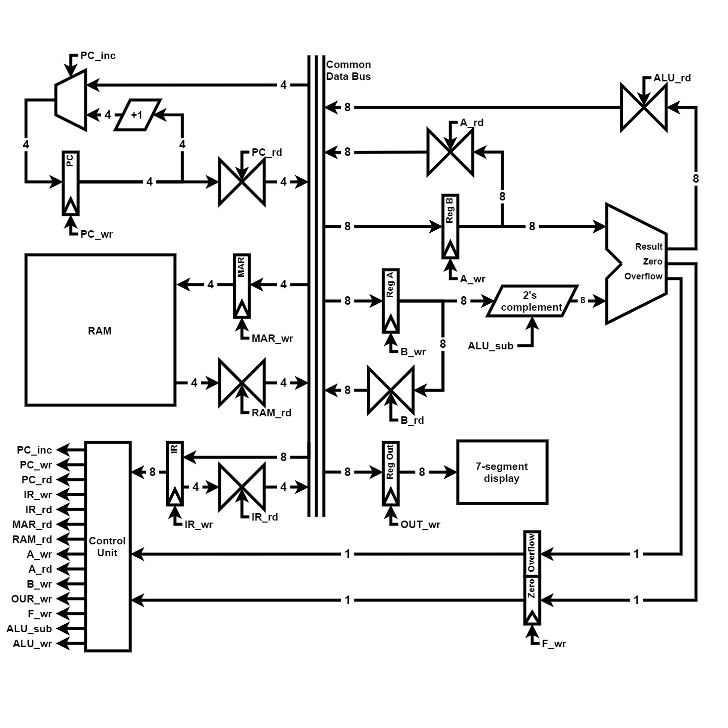
The instruction set presented by Malvino is very limited. Instructions are encoded into one byte, with 4 bits for the opcode and 4 bits for the operand. While it is enough to implement up to 16 instructions, Malvino only proposed 5 instructions : LDA, ADD, SUB, OUT and HLT which I will explain later. This instruction set doesn't even contain conditional and unconditional jumps or store instructions (it is not Turing complete).
Additionally, as RAM addresses are encoded on 4 bits, both the program and the data have to fit into 16 bytes. Hence, the SAP1 is closer to a Von Neumann architecture. The RAM is accessed through two registers : the Memory Address Register (MAR) is used to set which RAM address is read ; the Memory Data Register (MDR, W register, or RAM Out register) is used to access the value at the address pointed to by the MAR.
The SAP1 can perform additions and subtraction of unsigned 8-bit numbers. The two registers used for operations are the accumulator (register A) and the operand register (register B). A value can be directly written from RAM to the accumulator. When performing an arithmetic operation, the value of the operand is written to the B register, then the result of the ALU is written to the accumulator. The ALU implemented here is a simple ripple-carry adder. The third register is the Out register, used to display the result of calculations.
The Program Counter (PC) is incremented to read the next instruction. It can also be halted using the HLT instruction to stop execution of the program (when the result is calculated for instance). For each instruction, the Program Counter is used to read the instruction in RAM. The instruction is written to the Instruction Register (IR) where it is decoded.
All components are connected around the central bus which is used for every data transfer. For instance, to get a value from register A to register Out, register A is set to output its value on the bus and the register Out is set to read the value from the bus at the next rising edge of the clock cycle.
Execution of instructions is sequential and is performed in multiple steps (hence multiple cycles). In the original architecture, each instruction takes six steps to execute. The first three steps are common to each instruction and correspond to the Fetch sequence :
- T1 : MAR ← PC — The address of the next instruction is copied from the Program Counter to the Memory Address Register
- T2 : PC ← PC+1 — The value of the Program Counter is incremented for the next instruction
- T3 : IR ← RAM — The instruction at the correct RAM address is written to the Instruction Register
When the instruction is in the Instruction Register, the opcode is read and decoded. The correct sequence of control signals is emitted during the next three steps, T4, T5 and T6, this is the Execution sequence and depends on the instruction. The execution sequences for each instruction are detailed below alongside the instructions I added.
Improved SAP1
Malvino might have wanted to keep its architecture really as simple as possible. However, we can make a few modifications to make the processor more interesting.

SAP1 architecture
First, the execution cycle can be improved in two ways. During the fetch sequence, incrementing the Program Counter doesn't utilize the bus and therefore can be performed simultaneously with the third step. This reduces the fetch sequence from three to two cycles. Then, not all instructions require three cycles for their execution sequence. We can stop the execution at different steps for each instruction and avoid this waste.
And most importantly, we can add useful instructions to the instruction set. The main type of instruction missing are unconditional jumps and conditional branches. The latter require a condition depending on the result of the last operation of the ALU. Therefore, I added two flags : the Overflow and Zero flags. The flags are 1-bit registers updated after each operation of the ALU at the same time as the update of the Accumulator.
The other instruction I added are for convenience : load immediate, add immediate and subtract immediate with 4-bit value operand ; and compare and compare immediate to update the flags without changing the value of the Accumulator.
| Instruction | Mnemonic | Execution sequence |
|---|---|---|
| No operation | NOP | |
| Stop the processor | HLT | T3 : HLT |
| Load RAM to A | LDA |
T3 : MAR ← IR T4 : A ← RAM |
| Load immediate to A | LDA | T3 : A ← IR |
| Store A to RAM | STA |
T3 : MAR ← IR T4 : RAM ← A |
| Output result | OUT | T3 : OUT ← A |
| Add | ADD |
T3 : MAR ← IR T4 : B ← RAM T5 : A ← ALU & F ← ALU |
| Add immediate | ADI |
T3 : B ← IR T4 : A ← ALU & F ← ALU |
| Subtract | SUB |
T3 : MAR ← IR T4 : B ← RAM T5 : A ← ALU & F ← ALU |
| Subtract immediate | SUI |
T3 : B ← IR T4 : SUB & A ← ALU & F ← ALU |
| Compare | CMP |
T3 : MAR ← IR T4 : B ← RAM T5 : F ← ALU |
| Compare immediate | CMI |
T3 : B ← IR T4 : SUB & F ← ALU |
| Jump | JMP | T3 : PC ← IR |
| Branch if overflow | JIO | T3 : (OF flag) ? PC ← IR |
| Branch if zero | JIZ | T3 : (Z flag) ? PC ← IR |
Note that the instruction set is made of 15 instructions. This means we still have one opcode left for an additional instruction. However, I could not find an interesting instruction without adding a whole new component to the architecture.
Ternary SAP1
What's the point of using TernaryVerilog to implement a binary architecture ? So I also created a variant of the improved SAP1 using ternary logic.
This variant is a 6-trit processor working with 3-trit addresses. This allows for 27 lines of code instead of 16 for the binary version, and computation with signed numbers in the -364 to +364 range (instead of only unsigned values from 0 to 255). To be fully compatible, this variant has the same instruction set as the binary version. The opcode is encoded on three trits instead of four bits. Thus we could fit up to 27 instruction opcodes.
Ternary logic allows us to simplify the control signals, as well as change the zero flag to a sign flag. However, this is not used for the branch instructions.
The advantages of ternary logic cannot be appreciated just yet. A satisfying comparison would take into account power (simulating static and dynamic power consumption), performance (here only the range of values differs as the instruction set and execution sequences are the same) and area (simplified to the number of transistors). However, this requires a working circuit optimizer, as we saw in a previous article that a ternary ALU could be made faster and smaller through ternary algebra optimization.
Testbench
The secondary purpose of this project was to develop and test the TernaryVerilog testbench Python library. As stated in the previous article on the subject, it allows the user to initialize the processor and visualize the state of the processor while simulating it cycle by cycle.
Here are animations of the binary and ternary variants of the improved SAP1 architecture running a simple program to compute the Fibonacci sequence, simulated at 5Hz.
This article is part of my series of projects around Ternary Computing and Processor Design. Click here to see the list of projects of this series.
Go back to the list of projects